PCB Manufacturing
***NOTE*** This guide should be considered legacy or for those purely curious about the process of making PCB's or who need a copy of their prototype in an ultra short time frame, e.g. by tomorrow. the prototyping services of PCB manufacturers has become so competitive and cheap now that there is very little reason to etch your own anymore. Check the Getting PCBs Fabricated page for more info. ***END NOTE***
We have some basic PCB manufacturing kit available, which is suitable for small (approx 6x4 inches max) PCBs single and double sided. To date we have attempted only single sided boards. update to follow.
Precautions
This is a wet chemical process, and as such you need to use chemicals from or chemical cupboards:
Specifically please refer to chemical safety datasheets if unsure about the developer or etchant chemicals.
Materials required
- Chemicals
- Developer: Sodium MetaSilicate
- (Corrosive) pH>13 (strong alkaline) Dust from anhydrous form can cause respiratory burns, care whilst dissolving. Add powder to water. More detail later.
- Etchant: Sodium PerSulphate
- (Oxidising), (weak acid) harmful to eyes and skin, may combust in contact with low ignition point materials. Add powder to water and wear gloves!
- Water, simply from the tap.
- Containers
- Measuring cup (for water, when making developer solution)
- Small tray for developer solution
- Bigger tray for plain water
- Relatively large plastic box for heated water
- Smaller box for etchant, to place in heater water box
- Tools
- Laser printer
- UV light box
- Precision scale
- Optionally: (band)saw
- Optionally: files
- Optionally: PCB drill
- Optionally: Drill press
Note: You don't have to get these ready all at once, but it helps to make sure you know where everything is before getting started.
Print the design
- Design your PCB. A popular piece of software for this is Eagle.
- Ensure only the relevant layers are visible before printing the design. In the case of a single layer design, that's likely just the bottom layer + pads.
- Feed two transparent sheets into the laser printer, and print two black and white copies of the design on there.
- Cut out the PCB design to the same size from both sheets and align them perfectly. You need this because the black the laser printer produces isn't thick enough on a single copy. Use clear tape to attach the two sheets to one another, taking care not to have the tape cover the design.
 Eagle is an application you can use to design PCBs.
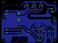 Only show the bottom layer and pads before printing the design.
 This is what you'll want to print on a transparent sheet.
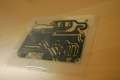 Aligned printouts taped together.
Prepare empty PCB
- Get some some photo etch single sided PCB, sometimes available in the space. If there is none available, Technobots sells it.
- Cut it to roughly the size of your design using a manual saw or the bandsaw.
- It's a good idea to leave some extra margin, to make it easier to handle during the developing and etching process.
 Saw your blank PCB to roughly the size of your PCB design.
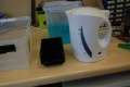
Prepare lighting and developing setup
- Gather the following items on a workbench:
- Gloves (put these on before starting to work with chemicals!)
- UV light box
- Measuring cup
- Small tray for developer solution
- Bigger tray for rinsing in water
- Developer (Sodium MetaSilicate)
- Scale
- Get 300ml of water from the tap with the measuring cup, and pour it into the small tray.
- Put the lid of the bottle of developer on the scale before turning it on. Pour 9g of developer into it. (3g of developer per 100ml of water).
- Pour into the small tray, and mix it up a bit with, for example, plastic tweezers you'll find where you find the trays. Make sure it's mostly dissolved.
- Fill the other tray with water.
- Put the scale and bottle of developer back where you found it.
If your empty PCB has enough of a margin, you can now drill a hole in there using the drill press. You can then, after lighting, route a plastic strap through there to make it easier to handle the PCB. Otherwise, you'll be using plastic tweezers to handle it instead.
 Wear gloves before all else.
 Pour 300ml of tap water into the small tray.
 Carefully measure out 9g of developer.
 Pour the developer into the tray; help it dissolve a bit by stirring with plastic tweezers.
Light and develop
- Peel the protective layer from the photo-sensitive side of your blank PCB.
- If you transparent print cutout matches the size of your empty PCB, fix the cutout the the photo-sensitive side of the blank PCB, making sure to get it in the right direction. Adding text to your design will likely help in getting this right. You can again use clear tape to attach the two.
- Place this combo copper-side down in the UV lightbox.
- For best results, fold some cardboard and place it on top of the PCB, for added pressure. This will make sure the design is pressed firmly to the PCB, and you won't get blurred edges.
- Close the lightbox tightly.
- Get a timer ready and set it for 3 minutes. Turn on the lightbox.
- Twiddle your thumbs for 3 minutes, perhaps give the developer solution another stir.
- After the 3 minutes are up, immediately turn off the lightbox and remove the PCB.
- Remove the transparent sheet from the PCB. You should see a faint shadow of your design in the photosensitive layer.
- If you've drilled a hole in the board, route a plastic strap through it now.
- Place the PCB in the developer solution, and move it around so the fluid moves across the surface.
- Keep a very close eye on it, as this is a quick process.
- After a short while, the parts of the UV-sensitive layer that were lit begin to dissolve, revealing the copper underneath it.
- Keep wiggling your board until all the UV-exposed parts look coppery.
- Once this is done, immediately place the PCB in the tray you filled with water, rinsing it.
- Your PCB is now developed.
 Peel the protective layer from your photo-sensitive blank PCB.
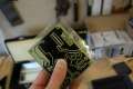 Align your transparent sheet printout with your blank PCB. Tape it together if necessary and viable.
 Place the PCB/transparent sheet combo face down in the UV lightbox
 You can add some folded cardboard on top, which will increase the pressure when the box is closed, resulting in a more focussed projection.
 Set a timer for 3 minutes immediately as you turn the lightbox on.
 After lighting, you should see a faint shadow of your design in the photosensitive layer.
 Immediately put the lit PCB into your developer solution.
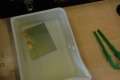 After a while, the lit parts of the UV-sensitive layer will start coming off, revealing a coppery colour (spoilers: it's copper).
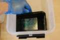
 When the PCB looks like this (all the UV-sensitive material that was lit dissolved), remove the PCB from the solution ASAP and rinse in water.
 The PCB is now ready for etching.
Tidy up lighting and development setup
- Pour the development solution into the water tray, diluting it.
- Pour this down the drain while the tap is running, diluting it a bit further.
- Wipe down both trays with some paper towel, and put them back where you found them.
- Return the lightbox, too.
Prepare etching setup
- Gather the following items on a workbench:
- Relatively large plastic box for heated water
- Smaller box for etchant, to place in heater water box
- Bottle of etchant solution
- Kettle
- Infra-red thermometer
- Add about a litre of cold water to your big plastic box
- Boil 1-1.5 litres of water with the kettle
- Pour hot water into big box, aim for a temperature of some 50°C.
- Pour a little bit of etchant solution in the small box, enough to submerge your PCB and still be able to move it around a little.
- Place etchant container into the big box, allowing the etchant to warm up.
 Gather a large plastic box, a smaller box for etchant, etchant solution, and a kettle.
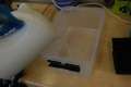 After adding a few centimetres of water in the large container, add boiling water with the kettle.
 Aim for a temperature of about 50°C
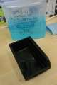 Pour a little bit of etchant in the small container
Etch the PCB
- Place the PCB into your warm etchant solution.
- Wiggle the PCB to get the etchant fluid moving across the surface.
- This will take about 30-35 minutes, depending on how strong the etchant is.
- After some 25 minutes, you will see copper starting to come of, this is the exciting part.
- Keep up the wiggling until all of the unwanted copper has gone.
- Rinse the etched PCB in water and wipe it dry.
- Your etch is now complete.
 After placing the etchant container in the hot water box and waiting for the etchant to warm up a while, place the developed PCB in the etchant solution.
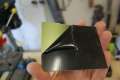
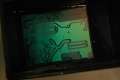 After about 25 minutes, copper will start to dissolve, revealing the colour of the board underneath.
 A better look at what the PCB looks like when it's partially etched.
 Another 10 minutes or so after that, all the UV-exposed parts will have dissolved. Remove the PCB from the etchant at that point.
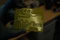 Rinse the PCB in water and dry it off. Your etch is now complete. The green colour to it will be removed after drilling, with acetone.
Tidy up the etching setup
- Pour the etchant solution back in its bottle, it can be used several more times.
- Pour out your warm water in the sink
- Rinse the container you used for etchant thoroughly
- Wipe both the big and small container with paper towel to dry them up; place them back on the shelf where you've found 'em.
- Put the etchant back in the chemicals cabinet.
Drill the PCB
Drill any component holes with correct sized drills. Test regularly with the actual components so you don't realise that your holes are too small when soldering.
TODO: more detail for the drilling setup
Wipe with acetone
Now the drilling is done, you should wipe the PCB with acetone and a paper a towel, revealing the nice coppery colour. Don't do this until right before you're planning to solder the PCB, to reduce oxidizing.
TODO: more detail, pictures
Place components and solder
You may want to use a flux pen on the pads for your components before soldering. Place your components according to your design and solder them. Done.
TODO: more detail, pictures
Data
| Board Type/Source | Mask Material | UV Exposure Type | UV Exposure Time | Developer Time | Etch Time | Result |
|---|---|---|---|---|---|---|
| RS - CIF AA16 | 2x OHP Transparency Laser Printed | old UV box | 4 mins | 25 mins | >30 mins | Slightly over-exposed, well developed, well etched. Good. |
| RS - CIF AA16 | 2x OHP Transparency Laser Printed | old UV box | 3 mins | 25 mins | >30 mins | Poor alignment. Under-exposed, over developed, well etched. Rubbish. |
| RS - CIF ABB20 | 2x OHP Transparency Laser Printed | old UV box | 4 mins | 22 mins | 33 mins | Correctly exposed and developed, well etched. Double sided! Huzzah! |
| my | board | here |
Potential future updates to this guide
- Double-sided process
- Better toolkit and relevant explanation/photos